The adverse phenomena and handling methods of Antminer S19 Pro during operation.
The adverse phenomena and handling methods of Antminer S19 Pro during operation.
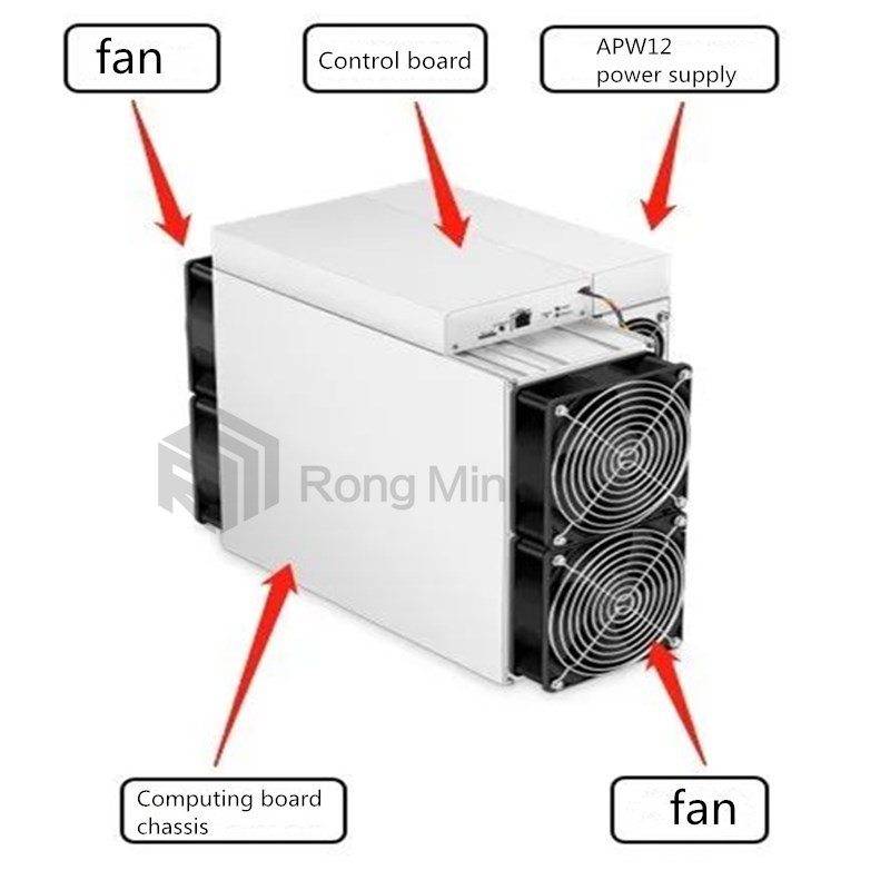
Hello everyone! I am Engineer Wang from Rongminer. First, let me introduce the overall architecture of the Antminer S19 Pro. The S19 Pro is mainly composed of 3 computing boards, 1 control board, APW12 power supply, and 4 cooling fans, as shown in the following figure:
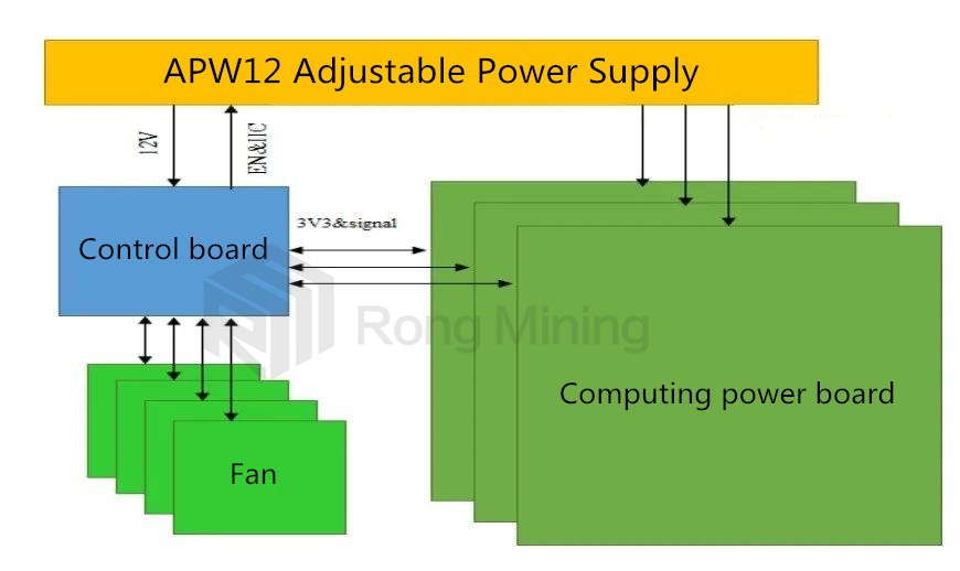
Next, let's take a look at the working structure of the S19 Pro's internal computing board
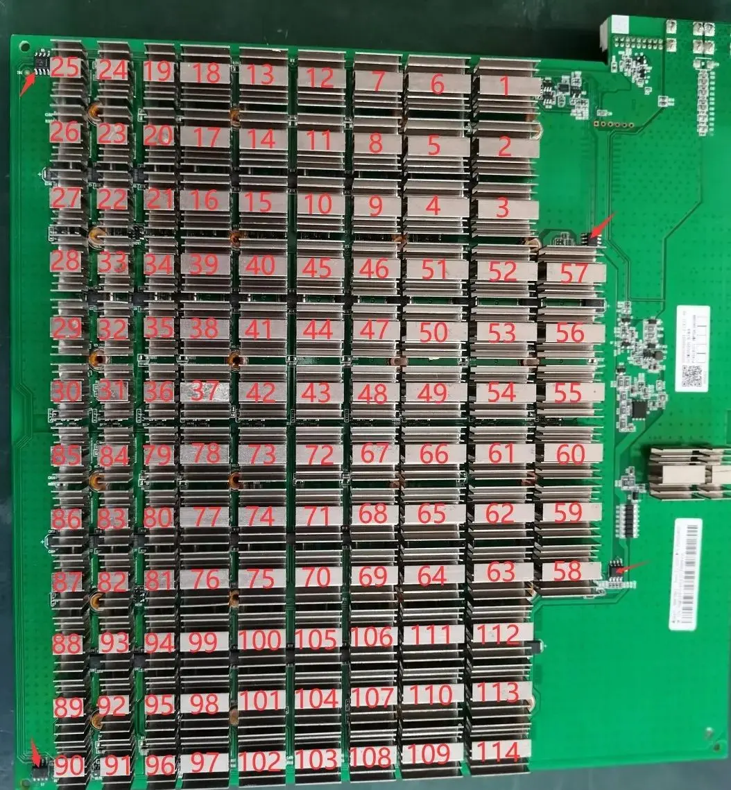
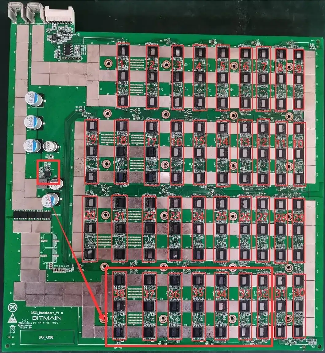
1. The Antminer S19 Pro computing board consists of 114 chips, divided into 38 groups (domains), each consisting of 3 ICs; The operating voltage of the S19 Pro chip is 0.32V; the 38th, 37th, 36th, 35th, 34th, 33rd, and 32nd groups (a total of 7 groups) are powered by 20V output from the boost circuit Q9 to output 1.8V to the LDO, and the 31st to 1st groups are powered by VDD 12.6V through the LDO to provide 1.8V. The voltage decreases by 0.32V for each backward domain.
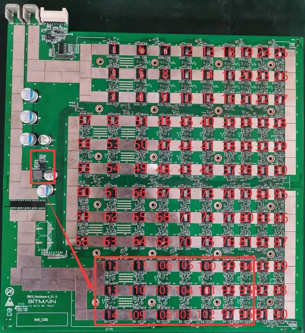
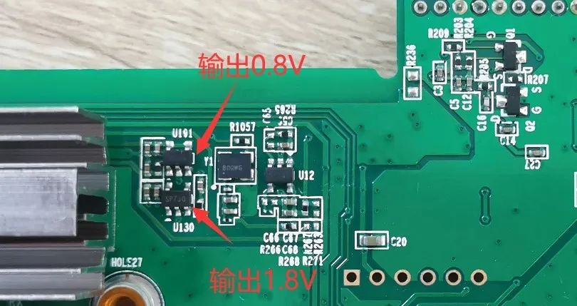
2. All 0.8V is provided by the local 1.8V output through LDO, as shown in the following figure:
In fact, after testing, the Antminer S19 Pro performs very well in terms of energy consumption ratio, stability, and other operating conditions under the officially recommended environmental conditions. If the computing board malfunctions, the most common phenomena include reporting 0, reporting numbers, and low computing power. In these situations, we can handle them this way——
(1). When the LCD display of the test fixture shows "ASIC NG: (0)", first measure the total voltage of the domain and the 20V boost circuit, and then use a short-circuit probe to short-circuit the RO test point and 1V8 test point between the first and second chips, and then run the chip finding program. Looking at the serial port log, if 0 chips are still found at this time, it will be one of the following situations:
a. Use a multimeter to measure whether the voltage at the 1V8 and 0V8 test points is 1.8V and 0.8V. If not, it may be an abnormality in the 1.8V and 0.8V LDO circuits of this domain, or the two ASIC chips in this domain are not soldered properly. Most of them are caused by short circuits in the 0.8V and 1.8V patch filter capacitors (measure the resistance values of the patch filter capacitors on the front and back of the PCBA);
b. Check whether the circuits of U2&U3&U4 are abnormal, such as resistance virtual soldering, etc;
c. Measure the resistance of R232 or R233 with a multimeter to see if it is within 1 ohm and the reading does not jump. If not, please replace these two resistors;
d.Check if there are any pins on the first chip that have not been soldered properly (it was discovered during maintenance that there is tin on the pins when viewed from the side, but when the chip was removed, it was found that the pins were not soldered at all.
(2). If one chip can be found in step 1, it means that the first chip and the previous circuit are both good. Use a similar method to troubleshoot the subsequent chips. For example, short circuit the 1V8 test point and RO test point between the 38th and 39th chips. If the log can find the 38 chips, then there is no problem with the first 38 chips; If 0 chips are still found, first check if the 1V8 is normal. If it is normal, then the chips after 38 have problems. Continue to use binary search until the problematic chip is found. Assuming there is a problem with the Nth chip, when the 1V8 and RO between the N-1 and Nth chips are short circuited, the N-1 chips can be found. However, when the 1V8 and RO between the Nth and N+1 chips are short circuited, the entire chip cannot be found.
(3). When the test fixture LCD displays "ASIC 113: (Report 113)", it indicates that the operation board can detect 114 chips at 115200 baud rate, but only 113 chips were found at 12M baud rate, and one chip was not found at 12M baud rate. Repair method: Using the binary method, short-circuit the 1V8 test point and RO test point between the 38th and 39th chips through a short-circuit probe. If the log can find the 38 chips, then the first 38 chips are fine; If there are 47 short circuits and the log reports 46, it means that the 47th chip cannot be detected and there is no problem with the appearance inspection. Generally, replacing the 47th chip is sufficient.
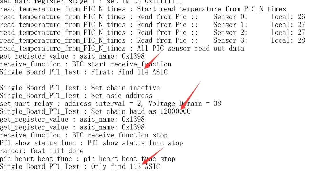
(4). When testing the fixture LCD display "ASIC NG: (X, fixed reporting of a certain chip)", there are two situations:
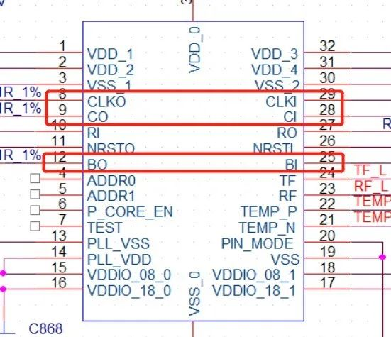
a. The first scenario; The testing time is basically the same as that of an OK board (usually the value of X does not change each time it is tested) (the testing time refers to the time from pressing the start testing button to the LCD displaying the result "ASIC NG: (X)"). This situation is most likely caused by abnormal soldering of the front and rear CLK, CI, and BO resistors of the Xth chip, so it is important to focus on these 6 resistors. The low probability is due to abnormal soldering of the following pins in the X-1, X, and X+1 chips:
(b). The second scenario; The testing time is almost twice as long as that of the OK board (sometimes the X value may change during each test, and sometimes X=0); At this time, the log usually contains the following information (the red number may not necessarily be 13, depending on which socket the wiring harness is connected to); During testing, it is assumed that the domain voltages of almost all domains in front of the abnormal position are less than 0.3V, and the domain voltages of the rear domain are almost all higher than 0.34V. This situation is caused by the chip not being soldered properly, usually 1.8V, 0.8V, RXT, CLK are not soldered properly. Suggest directly measuring the domain voltage to locate where the problem is occurring. The 1V8 and RO short-circuit methods used in step 1 can also locate the location of the anomaly.

(c). At present, most of the maintenance experience has found micro short circuits (0-several hundred ohms) between signals, which are caused by the low resistance of chip pins. You can first use a hot air gun to solder and see if it is OK.
(5). If the computing power of a single board is low, here is a convenient and quick method to locate and repair it - that is, log in to the IP through Putty software to observe whether the domain working voltage and NONCE return of this board are normal, and repair it according to Putty's log information.
The specific operation is as follows:
(1). Open the IP address of the machine with input issues and click OPEN
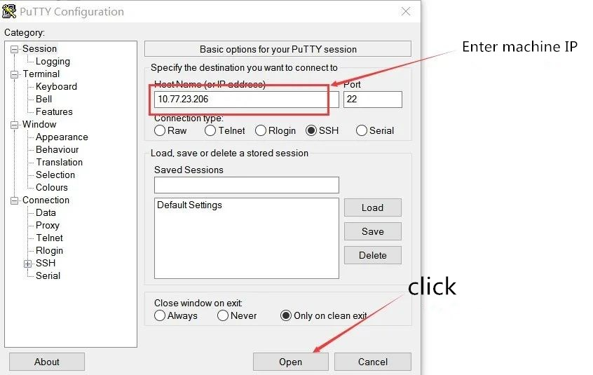
(2). By entering the username, password, and test command, you can see the status of NONCE return and voltage domain. If there are abnormal conditions in NONCE and domain voltage, you can measure and repair based on the printed abnormal chip.

Finally, I would like to share with you a repair process, hoping to provide help for everyone's thinking when repairing mining machines:
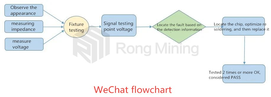
The above is my engineer's quality analysis and processing method for the S19 machine. If you have any questions, you can consult us
Follow 'Rongbtc '
Rongbtc constantly recommends new Asic Miners Asic Miner Power Supply、Asic Miner Water Cooling Plate、 Asic Miner Control Boar、 Asic Miner FAN 、 Asic Miner Chips, Provide the best products for every miner and create more value!


